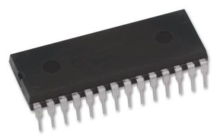
The ATTINY48-PU is a low-power 8-bit CMOS Microcontroller based on the AVR enhanced RISC architecture. By executing powerful instructions in a single clock cycle, the ATtiny48 achieves throughputs approaching 1MIPS per MHz allowing the system designer to optimize power consumption versus processing speed. The AVR core combines a rich instruction set with 32 general purpose working registers. All the 32 registers are directly connected to the arithmetic logic unit (ALU), allowing two independent registers to be accessed in one single instruction executed in one clock cycle. The resulting architecture is more code efficient while achieving throughputs up to ten times faster than conventional CISC microcontrollers. The ATtiny48 provides 4kB of in-system programmable flash, 64byte EEPROM and 256byte SRAM. The device achieves up to 12MIPS throughput at 12MHz.
Advanced RISC architecture
123 Powerful instructions most single clock cycle execution
32 x 8 General purpose working registers
Fully static operation
One 8-bit timer/counter with separate prescaler and compare mode
One 16-bit timer/counter with prescaler and compare and capture modes
Master/Slave SPI serial interface
Byte-oriented 2-wire serial interface (Philips I2C compatible)
Programmable watchdog timer with separate on-chip oscillator
On-chip analog comparator
Interrupt and wake-up on pin change
DebugWIRE on-chip debug system
In-system programmable via SPI port
Power-on reset and programmable brown-out detection
Internal calibrated oscillator
External and internal interrupt sources
Three sleep modes - Idle, ADC noise reduction and power-down
On-chip temperature sensor
240μA at 1.8V (1MHz System Clock) Active mode power consumption