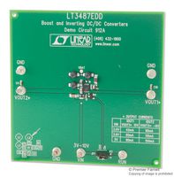
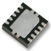
The DC912A demonstration circuit features LT3487EDD regulator. The LT3487EDD is a dual channel switching regulator generates positive and negative outputs for biasing CCD imagers. The demo circuit demonstrates small size and low component count in a boost circuit and an Inverting circuit. The boost converter is designed to convert a 3V to 5V input to 15V output at 45mA to 90mA maximum load. The inverting circuit generates a -8V output at 90mA to 150mA maximum load from the same input. Since the maximum VIN of the LT3487EDD is 16V, this demo circuit will work well at higher inputs. The only limitation is that the input has to be lower than the boost converter output (15V) in order to stay in regulation. If Vin and VBAT will be powered separately, cut trace as indicated on farside of board and use ?VBAT? pad on top.
- 70% efficiency
- Output disconnect
- Positive output reaches regulation before negative channel begins switching
- Internal schottky diodes
- Requires only one resistor per channel to set output voltage
- Short circuit robust
- Capacitor programmable soft start
- Separate VBAT pin allows separate sources for power and control circuitry
电源管理, 成像, 视频和目视