S29JL032J70TFI320,1972451,闪存, 32 Mbit, 2M x 16位 / 4M x 8位, CFI, TSOP, 48 引脚,CYPRESS SEMICONDUCTOR
laird代理商
专业代理销售laird(莱尔德)全系列产品-新加坡2号仓库
美国1号分类选型新加坡2号分类选型英国10号分类选型英国2号分类选型日本5号分类选型

在本站结果里搜索:    
热门搜索词:28B0500-100  IRF9540  保险丝  amphenol  4.7μF 63V 5mm  P沟道 8ohm SOT-23  2581138

S29JL032J70TFI320 - 

闪存, 32 Mbit, 2M x 16位 / 4M x 8位, CFI, TSOP, 48 引脚

CYPRESS SEMICONDUCTOR S29JL032J70TFI320
声明:图片仅供参考,请以实物为准!
制造商产品编号:
S29JL032J70TFI320
仓库库存编号:
1972451
技术数据表:
(EN)
订购热线: 400-900-3095  0755-21000796, QQ:800152669, Email:sales@szcwdz.com
由于产品数据库庞大,部分产品信息可能未能及时更新,下单前请与销售人员确认好实时在库数量,谢谢合作!

S29JL032J70TFI320产品概述

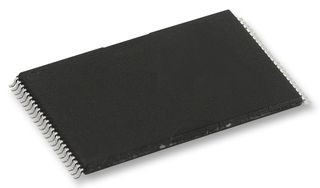
The S29JL032J70TFI320 is a 32MB simultaneous Read/Write Flash Memory organized as 2097152 words of 16-bit each or 4194304 bytes of 8-bit each. Word mode data appears on DQ15-DQ0, byte mode data appears on DQ7-DQ0. The device is designed to be programmed in-system with the standard 3V VCC supply and can also be programmed in standard EPROM programmers. The device is available with an access time of 70ns. Standard control pins - chip enable (CE#), write enable (WE#) and output enable (OE#) - control normal read and write operations and avoid bus contention issues. The device requires only a single 3V power supply for both read and write functions. Internally generated and regulated voltages are provided for the program and erase operations.
  • Bottom boot device, 2 banks - 8/24MB
  • Data can be continuously read from one bank while executing erase/program functions in another bank
  • Zero latency between read and write operations
  • Multiple bank architecture
  • Manufactured on 0.11μm process technology
  • Zero power operation
  • Compatible with JEDEC standards
  • Pinout and software compatible with single-power-supply flash standard
  • Cycling endurance - 1million cycles per sector typical
  • Data retention - 20 years typical
  • Supports common flash memory interface
  • Erase suspend/erase resume
  • Data# polling and toggle bits
  • Provides a software method of detecting the status of program or erase operations
  • Unlock bypass program command - Reduces overall programming time
  • Ready/busy# output - Hardware method for detecting program or erase cycle completion
  • Hardware reset pin - Hardware method of resetting the internal state machine to the read mode
  • WP#/ACC input pin - Acceleration function accelerates program timing
  • Write protect function protects the two outermost boot sectors regardless of sector protect status
  • Hardware method to prevent any program or erase operation within a sector

计算机和计算机周边, 工业, 通信与网络, 消费电子产品

S29JL032J70TFI320产品信息

  存储器容量  32Mbit  
  闪存配置  2M x 16位 / 4M x 8位  
  时钟频率  -  
  芯片接口类型  CFI  
  封装类型  TSOP  
  针脚数  48引脚  
  存取时间  70ns  
  电源电压最小值  2.7V  
  电源电压最大值  3.6V  
  工作温度最小值  -40°C  
  工作温度最高值  85°C  
  封装  每个  
  产品范围  3V Parallel NOR Flash Memories  
  MSL  MSL 3 - 168小时  
关键词         

S29JL032J70TFI320相关搜索

存储器容量 32Mbit  CYPRESS SEMICONDUCTOR 存储器容量 32Mbit  闪存 存储器容量 32Mbit  CYPRESS SEMICONDUCTOR 闪存 存储器容量 32Mbit   闪存配置 2M x 16位 / 4M x 8位  CYPRESS SEMICONDUCTOR 闪存配置 2M x 16位 / 4M x 8位  闪存 闪存配置 2M x 16位 / 4M x 8位  CYPRESS SEMICONDUCTOR 闪存 闪存配置 2M x 16位 / 4M x 8位   时钟频率 -  CYPRESS SEMICONDUCTOR 时钟频率 -  闪存 时钟频率 -  CYPRESS SEMICONDUCTOR 闪存 时钟频率 -   芯片接口类型 CFI  CYPRESS SEMICONDUCTOR 芯片接口类型 CFI  闪存 芯片接口类型 CFI  CYPRESS SEMICONDUCTOR 闪存 芯片接口类型 CFI   封装类型 TSOP  CYPRESS SEMICONDUCTOR 封装类型 TSOP  闪存 封装类型 TSOP  CYPRESS SEMICONDUCTOR 闪存 封装类型 TSOP   针脚数 48引脚  CYPRESS SEMICONDUCTOR 针脚数 48引脚  闪存 针脚数 48引脚  CYPRESS SEMICONDUCTOR 闪存 针脚数 48引脚   存取时间 70ns  CYPRESS SEMICONDUCTOR 存取时间 70ns  闪存 存取时间 70ns  CYPRESS SEMICONDUCTOR 闪存 存取时间 70ns   电源电压最小值 2.7V  CYPRESS SEMICONDUCTOR 电源电压最小值 2.7V  闪存 电源电压最小值 2.7V  CYPRESS SEMICONDUCTOR 闪存 电源电压最小值 2.7V   电源电压最大值 3.6V  CYPRESS SEMICONDUCTOR 电源电压最大值 3.6V  闪存 电源电压最大值 3.6V  CYPRESS SEMICONDUCTOR 闪存 电源电压最大值 3.6V   工作温度最小值 -40°C  CYPRESS SEMICONDUCTOR 工作温度最小值 -40°C  闪存 工作温度最小值 -40°C  CYPRESS SEMICONDUCTOR 闪存 工作温度最小值 -40°C   工作温度最高值 85°C  CYPRESS SEMICONDUCTOR 工作温度最高值 85°C  闪存 工作温度最高值 85°C  CYPRESS SEMICONDUCTOR 闪存 工作温度最高值 85°C   封装 每个  CYPRESS SEMICONDUCTOR 封装 每个  闪存 封装 每个  CYPRESS SEMICONDUCTOR 闪存 封装 每个   产品范围 3V Parallel NOR Flash Memories  CYPRESS SEMICONDUCTOR 产品范围 3V Parallel NOR Flash Memories  闪存 产品范围 3V Parallel NOR Flash Memories  CYPRESS SEMICONDUCTOR 闪存 产品范围 3V Parallel NOR Flash Memories   MSL MSL 3 - 168小时  CYPRESS SEMICONDUCTOR MSL MSL 3 - 168小时  闪存 MSL MSL 3 - 168小时  CYPRESS SEMICONDUCTOR 闪存 MSL MSL 3 - 168小时  
电话:400-900-3095
QQ:800152669

S29JL032J70TFI320产地与重量

原产地:
Thailand

进行最后一道重要生产流程所在的国家

RoHS 合规:
税则号:
85423261
重量(千克):
.002939
laird电子简介 | laird产品 | laird动态 | 按系列选型 | 按产品规格选型 | laird产品应用 | laird选型手册
Copyright © 2017 www.laird-tek.com All Rights Reserved. 技术支持:电子元器件 ICP备案证书号:粤ICP备11103613号
版权所有:深圳市创唯电子有限公司 客服电话:400-900-3095 企业QQ:800152669 邮箱:sales@szcwdz.com